Google's TPUv8
April 22, 2026
Today, Google announced their eighth-generation TPUs: a training/RL (8t) and inference (8i) chip. I’m grateful that they shifted away from the efficiency/performance epithets - t/i seems to capture the same distinctions (i.e., inference should be performant and power efficient) but in a much more direct manner. Their seventh generation Ironwood (7x) seemed pretty eclectic and catch-all, marketed for both “large-scale AI training and inference” as well as “dense and MoE models.”1 The last generation to feature two chip variants was v5(e/p), and this might substantiate the rumors that the 7x was initially intended to be the “v6p”, likely a training chip. That said, they did announce it as the “TPU for the age of inference.”2 To chart the trajectory more firmly, we have
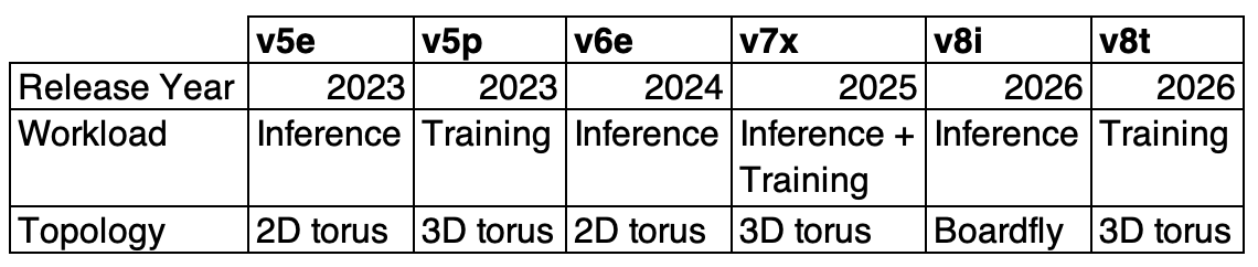
The rhythm of the inference/training variants is interrupted with this new announcement: v8i’s Boardfly topology is super exciting and certainly a stand out. It’s coupled with their Virgo network and answers a ton of questions I had about their scale-out network for multi-slice (maybe now just multi-pod?) communication. We’ll get to this below.
To structure this post, I want to first capture some of the important details from the initial announcement and then stage a Joyce-esque catechism (Q/A format) to relate how some of my outstanding questions have been answered (or remain unanswered).
While previous generations of TPUs staggered the releases of their variants, v8 launched the inference and training chips simultaneously. There’s also an interesting story to be read in the provenance of these chips: 8t (Sunfish) was produced in collaboration with Broadcomm while 8i (Zebrafish) was produced with MediaTek, but only in a limited capacity to supplement the areas where Google didn’t have as much expertise.3 There has been recent news about Marvell collaborating with Google on their TPUs, suggesting either a gradual shift in the Google’s semiconductor supply chain, or more generally the importance of supply chain diversity.
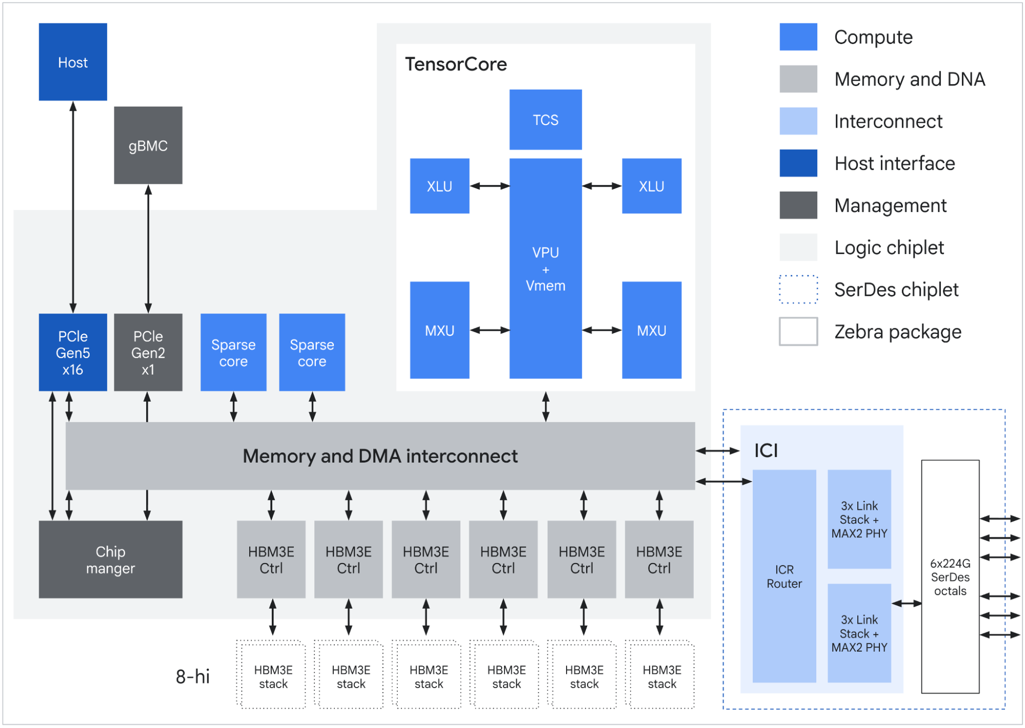
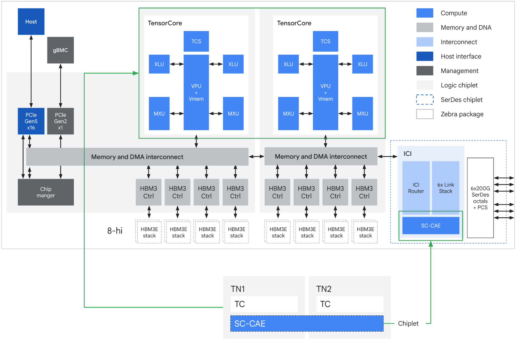
The biggest headline is the 3x increase in on-chip SRAM in comparison to the previous Ironwood generation. Other than that, the main evolution on the silicon might be the Collectives Acceleration Engine (CAE) on the 8i.
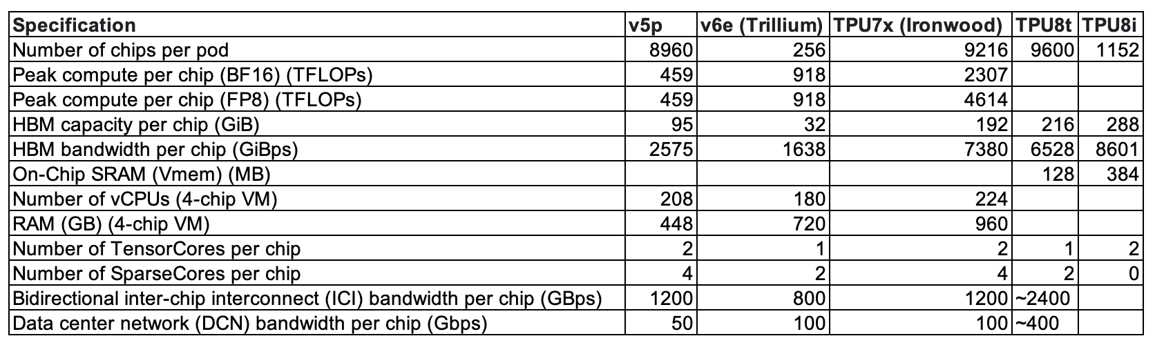
The one CAE chiplet replaces the 4 SparseCores featured on Ironwood. The SparseCore was introduced in the TPUv4 paper as a way to alleviate the cost of interacting with embeddings on the TensorCore, which is optimized for dense operations. Doing so on tensor cores would be “suboptimal due to small gather/scatter memory accesses”4 and the CAE accelerates “reduction and synchronization steps,”5 so I’m unsure whether the shift away from the SparseCore to CAE is more of a naming departure or a shift in the silicon (other than a reduction in chiplet count).
Apart from the presence/lack thereof of the CAE, the two chips doesn’t seem too different (we’ll get to topology in a moment). 8i has more HBM capacity and BW, an additional TC, and a lot more SRAM. The emphasis on SRAM echoes Nvidia’s acquisition of Groq and their LPUs - not a shift to, but rather an investment in, workloads optimizing for latency over throughput. The host CPU for both systems is their ARM Axion, but we don’t seem to have details beyond that. One last note is that Google’s TPUs still make use of 224G SerDes, whereas Nvidia recently announced a 400G SerDes for their Vera Rubin systems.
Boardfly is probably the most interesting thing to come out of this announcement. For generations, inference/efficiency chips were networked in a 2D torus. For the 6e, one host CPU connected to 8 TPUs and while every TPU thus has a PCIe link directly to the host, the chips are not networked in an all-to-all manner. In a 4x4 topology, it would take an additional 2 hops to get from top to bottom, or 5 hops to cross the entire diameter (vs. no additional hops in an all-to-all topology). This can be mitigated, to a degree, with wraparounds which are available when the rank is the full 16 chips (16x16, for instance).
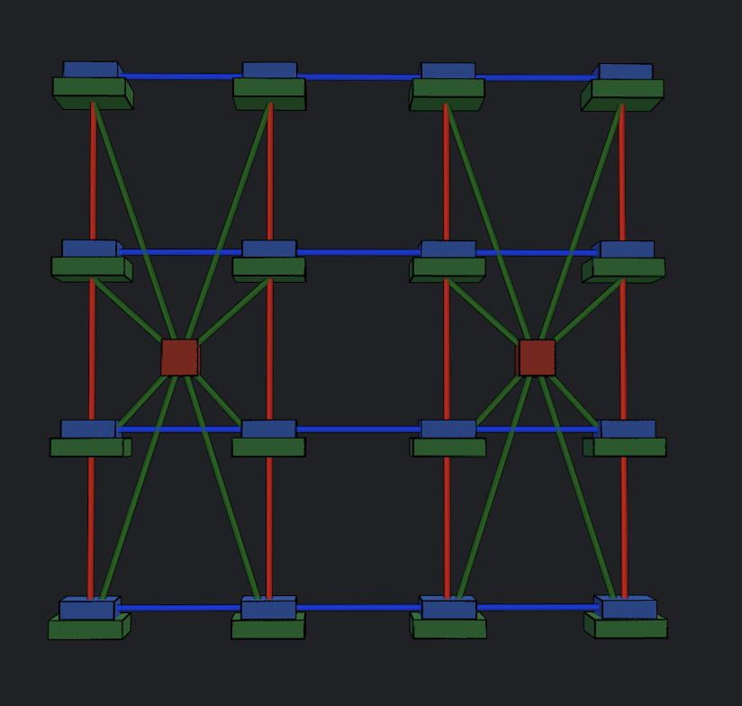
With Boardfly, TPUs on a tray, or a building block (BB), are connected all-to-all. Then, groups use copper DACs to connect 8 BBs together. This uses “11 of the available external links”, but I’m unclear what this looks like exactly, and what the aggregate bandwidth within a group might be. It seems as though they utilize TPU-to-TPU links, with the TPUs just being located in different BBs. This would mean intra-group communication would have to hop through TPUs. Finally, a pod is up to 36 groups connected via OCS, but there are not many details there either.
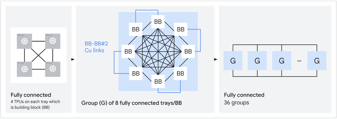
The world-size of the inference chip has greatly improved to 1,152. Maybe serving MoEs can better make use of this new topology and world-size as opposed to dense models, where parallelism might be bottlenecked by the KV heads.
Between generations of hardware we sometimes see crazy improvements, like 30x or 100x, and it certainly doesn’t help when the numbers are inflated. That said, the introduction of TPUDirect RDMA seems to be a massive leap forward for compute efficiency. I had just asked this question into the X void:
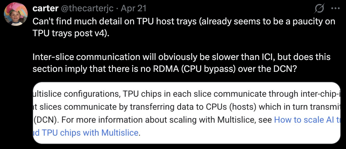
For intra-slice communication, there wouldn’t be a need for RDMA since the scale-up/ICI network would be used over the scale-out/backend network, typically a RoCE or IB fabric. For ICI communication, the TPU would send information to the ICI egress, bypassing the PCIe link to the host tray. For inter-slice communication, traffic needs to traverse the scale-out network and travels from the TPU’s HBM over the PCIe bus to the host CPU, then out the egress there. RDMA-enabled traffic still needs to travel over the slow PCIe lane, but can skip the host CPU (which is slow). I don’t have a good source to relate this to and quantify the potential performance gain, but pretty much all DCNs for AI workloads use an RDMA enabled fabric - Gangidi’s Meta paper is an excellent read on this topic. I am not sure whether TPUDirect RDMA is truly new or not, but would be surprised if it was.
In the vein of scale-out network details, it was cool to see more information about their Virgo Network design but it wasn’t terribly informative. The two big takeaways were that (1) they use a 2-layer Clos topology not unlike what we’ve seen before, and (2) Virgo encompasses hetergenous accelerators (GPUs and TPUs). Google has entered into an agreement with Nvidia to purchase up to 960,000 Rubin GPUs, which would have to require up to 1.5GW of capacity.6 It is pretty neat to see Google buy into hardware heterogeneity. Obviously, this capacity would quickly be purchased through Cloud, but I’m curious whether internal teams use GPUs or if it is primarily TPU-only. They also announced that Pytorch native support for TPUs is now in preview, so I’m curious how difficult it is to train a single model/task on different accelerators, and also across generations.
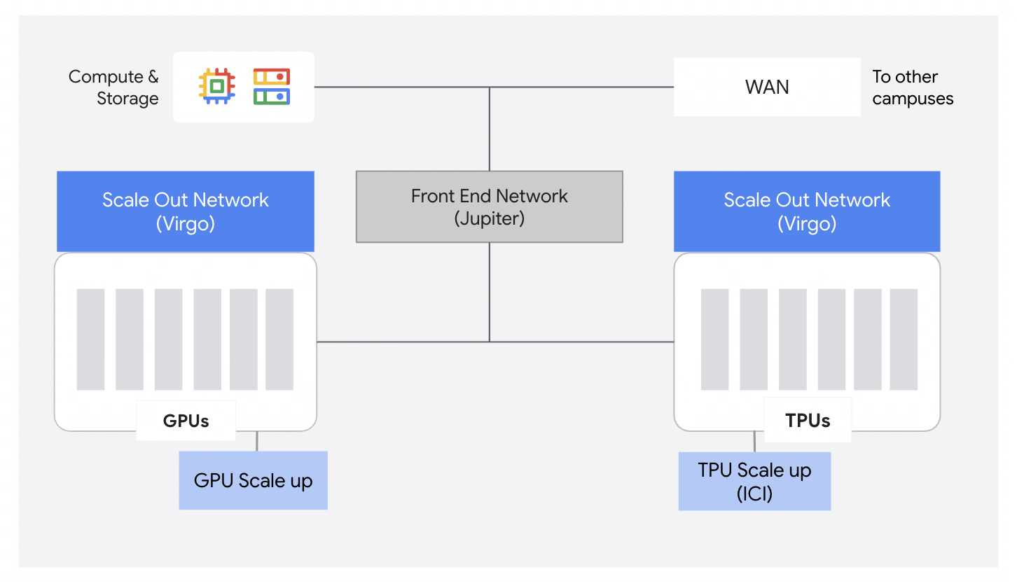
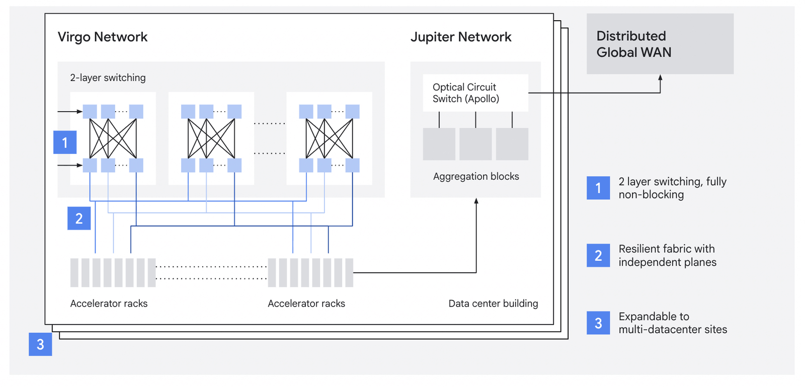
I hadn’t seen much information about their DCN for AI workloads prior to this announcement, so the confirmation that they use a 2-tiered Clos-like topology solidifies the fact that they use electronic packet switching (EPS) rather than OCS for the leaf/spine. Moreover, uou can see that Jupiter (OCS) is still being used for the frontend network, and that there is no aggregation layer to connect the spines. I am curious whether there is an aggregation layer at all (they talk about 1mil+ node clusters, so I imagine there is) and whether it uses OCS over another electronic switch.
As for the questions, I’ll keep the answers relatively brief. I’m wrapping up another post that will go into many aspects of the ICI and DCN in more detail.
What are the limitations of a 3D torus for training, and a 2D torus for inference? How does ICI topology compare to NVLink?
This is by far the most interesting question. Obviously, in comparison to an all-to-all topology like with NVLink, communication between two arbitrary TPUs in a pod will incur more latency (more hops) on average. Wraparounds and twisted topologies can reduce this cost, and neighbor-to-neighbor communication remains fast, but this is an inherent limitation that can bottleneck certain communication patterns, like the all-reduces required for tensor and data parallelism.
I am not certain why previous inference chips used a 2D torus topology. If I were to hypothesize, I would look to the “efficiency” epithet: maybe it was just for cost reasons. Indeed, both 3D and 2D toruses are cheaper (less transceivers/copper) than an all-to-all design. Furthermore, parallelizing dense models like Llama3 might be limited by the degree of the KV heads, so a 3D torus topology might have not been necessary for common inference deployments. That said, MoE has been de-facto for some time now, so I’m not sure how well this holds. The shift to the radix/Dragonfly topology seems to reflect changing inference workloads. That said, I’m not confident on the details yet, so I will leave this question for now, with the intent to revisit it and gather some empirical evidence to found my next answer.
How does the scale-out network look? How would data flow from the TPU, across the DCN, to the destination TPU?
We received a firm answer to this end (maybe with a few details occluded). Their scale-out/backend network, Virgo, is a 2-tier Clos-like topology (non-blocking, leaf/spine). Jupiter, which uses OCS, is still used for frontend networking. The promotional diagrams elided any aggregation level switch, but I’m curious whether this could make use of Jupiter and/or OCS - or whether they decided to not have an aggregation layer at all. Judging from their intended scale, this would surprise me.
So, when TPUs need to communicate beyond the ICI and over the scale-out network, data will be transfered from the TPU HBM, over PCIe to the host, and out the egress NIC (to be mirrored at the destination). Critically, data does not need to travel through the host CPU because of the introduction of TPUDirect RDMA (like the GPUDirect RDMA counterpart) and the fact that Virgo must be running RoCEv2.
How does Google’s DCN compare to other hyperscaler designs?
As mentioned above, Gangidi at Meta has a really good paper on their AI DCN design and use of RDMA. Comparing their two designs reveals that they are remarkably similar, i.e. a 2-tiered Clos-like topology.
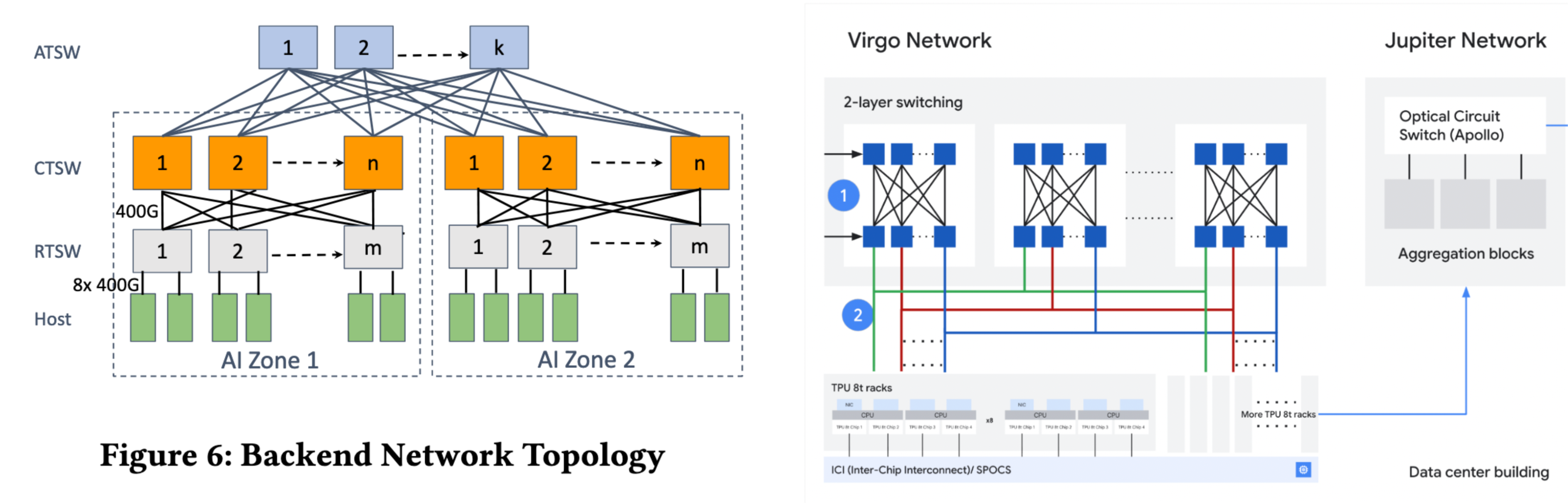
Meta makes use of an aggregation layer for communication between their “AI Zones” (which seems like it can be a spatial designation too), where Google does not mention the same. That said, the similarity between the two designs makes me wonder what kind of topology diversity there is between different hyperscalers, or whether the designs have largely converged. However, even if top-level designs have converged, the devil is always in the detail (implementation).
What does the host tray on a TPU rack look like?
To my knowledge, there still isn’t a good source on this matter. We have seen pictures of TPU trays though.
What was the DCN before Virgo? EPS or OPS?
Unfortunately, I don’t know the question to this either. We know that Google supported multi-slice training (and potentially inference? why not) before this, which necessitates DCN traversal beyond the pod size, but it seems unclear whether this was different than the announced Virgo Network. Based on their scaling book, it does seem like the introduction of TPUDirect RDMA is new and I’m unsure what would have impeded an earlier rollout.
I am always excited to hear more news directly from the source; that said, as the AI ‘race’ continues to heat up, it’s sad to see the amount of information we get become sparser. Maybe more details will emerge about v8, but a lot of the interesting figures were either elided or defined relationally (2x the previous generation, etc). The details about the CAE seemed to be concealed with marketing-tongue, and I was left wanting to know a lot more about the Virgo network. The TPUv4 paper was published in 2023. I referenced Meta’s RDMA paper which was from 2024. Will we continue to see these organizations become increasingly tight-lipped? Some of the best recent sources of information have been from Chinese labs (like Moonshot), not American ones. I write from an outside perspective and wonder if there are any networks between these companies that facilitate the transfer of info, though I doubt it. Maybe Nvidia doesn’t care if you achieve an optimal MFU on their NVL72, but just that it performs better than a competitor’s offering. Cloud computing has always been in the business of optimizing everything, so it makes sense to keep secrets close. Maybe things will change, or maybe we’ll get some more information once a few years elapse.
It was very timely to see their shift to the Boardfly topology for the inference chip. I wasn’t wowed by the silicon of the 8i (although maybe the cool details are occluded), so the interconnect really stood out. I’m less familiar with the Dragonfly topology and its use in the Cray platform, but I am curious whether we’ll see system providers like Nvidia converge on a design that is not necessarily all-to-all. That said, the split between switched and toroidal still seems to be pronounced since the 8t retains the 3D torus topology.
Google’s positioning as an end-to-end system provider, from silicon to DC, cannot be understated. It’s consistently impressive to see their advancements, and although TPUv8 certainly doesn’t seem to be a ‘Nvidia-killer’, I’m really excited to see the continued emphasis on scale-up and scale-out networking.
-
https://blog.google/innovation-and-ai/infrastructure-and-cloud/google-cloud/ironwood-tpu-age-of-inference/ ↩︎
-
https://www.techpowerup.com/343957/google-prepares-tpuv8ax-for-training-and-tpuv8x-for-inference ↩︎
-
https://cloud.google.com/blog/products/compute/tpu-8t-and-tpu-8i-technical-deep-dive ↩︎
-
https://blogs.nvidia.com/blog/google-cloud-agentic-physical-ai-factories/?ncid=so-twit-202209&linkId=100000418840792 ↩︎